


 Download Free Sample
 Buy Now
Market Size
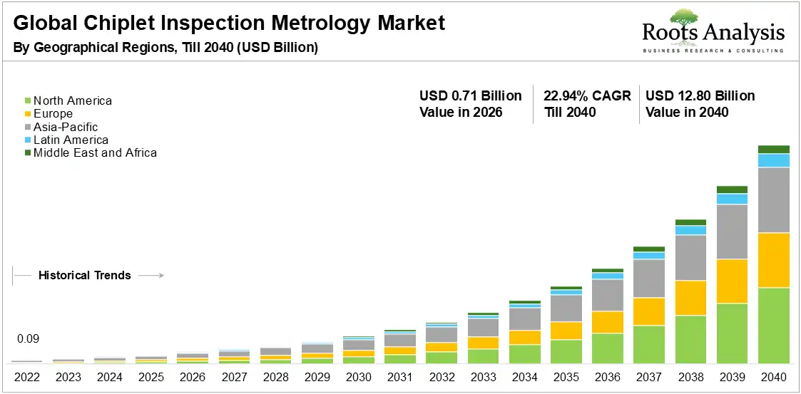
The global chiplet inspection metrology market is projected to reach USD 0.71 billion in 2026 and USD 12.80 billion by 2040, representing a CAGR of 22.94% during the forecast period 2026 to 2040.
See What’s in the Full Report – Request Your Complimentary Insights!
Market Overview
The chiplet inspection metrology market includes precision measurement systems used to verify the physical quality and integrity of individual chiplets and their subsequent integration into advanced package assemblies. The market scope encompasses inspection equipment for critical process steps, including die-to-die alignment verification, interposer inspection, through-silicon via (TSV) analysis, and hybrid bonding quality control. Value is created by ensuring reliable connections and high manufacturing yields in heterogeneous integration, which is essential for developing high-performance computing (HPC) and artificial intelligence (AI) accelerators.
Market expansion is primarily driven by the limitations of traditional monolithic scaling (Moore's Law) and the resulting shift toward modular and advanced packaging architectures. Demand for sophisticated inspection tools is particularly acute in end-use sectors like high-performance computing, data centers, and automotive electronics, where device reliability and power efficiency are paramount. This trend gained significant commercial momentum when the Universal Chiplet Interconnect Express (UCIe) Consortium published its 1.0 specification in early 2022. This standardization effort accelerated the commercial viability of multi-vendor chiplet ecosystems, driving demand for new metrology solutions to verify interoperability and physical connections.
Innovation in the sector is focused on integrating artificial intelligence and machine learning algorithms into inspection tools to improve defect detection accuracy and throughput for increasingly complex 3D stacking and hybrid bonding processes. Non-destructive testing methods are also gaining importance, minimizing damage during inspection while maximizing data insights. This trend indicates a strong shift toward highly automated, inline metrology solutions to support volume manufacturing. The market outlook is positive, underpinned by sustained investment in next-generation advanced packaging technologies across the semiconductor value chain.
Market Report: Key Takeaways
- Leading Players in Chiplet Inspection Metrology Industry: Top tier companies, such as Applied Materials, Camtek, Hitachi High-Tech, Onto Innovation, EV Group, Omron, and Keyence are widely emphasizing integrated solutions, packaging-to-front-end workflow optimization, and silicon photonics integration in chiplet packages. Based on our 2.5 D / 3D packaging metrology market research, KLA invested USD 138 million to expand its advanced packaging metrology portfolio to capture 2.5D /3D inspection growth.
- Startup Ecosystem: New cohort of startups is introducing radical new modalities for chiplet inspection. Key players like Nearfield Instruments pushing the boundaries of atomic force microscopy (AFM), Nearfield’s multi-probe systems address the throughput limitations of traditional scanning probe metrology. Their partnership with IMEC and recent EUR 135 million funding round position them as a major player in the 3D metrology space.
- Funding and Investment Analysis: The advanced packaging metrology market analysis highlights that the industry is backed by robust funds and investments to accelerate the development of advanced chiplet inspection metrology. In April 2025, Wooptix secured €10.0 million in Series C funding round led by Samsung Venture, Intel Capital, and TEL Venture Capital Society of Spain. The company says that its wavefront phase is imaging for blank / patterned wafer-shape measurement with sub-nanometer heigh resolution. Currently, company offers manually operated 200mm and 300mm wafer metrology tools and is planning to introduce a fully automated tool.
- Major Market Pull: The development of advanced silicon and glass interposers for 2.5D and 3D integration requires highly precise inspection during fabrication. As these interposers form the foundation of the chiplet package, accurate metrology for through-silicon vias (TSVs), micro-bumps, and routing lines offers a distinct market opportunity separate from die-level inspection.
Recent Industry Developments
- In January 2026, TSMC announced to begin volume production of 2nm-class GAA transistor, featuring first-generation nanosheet transistor technology for TSMC claiming up to 15% improvement at ISO power.
- In December 2025, QuantumDiamonds (a Munich-based quantum sensing startup company) unveiled its plan to invest €152 million to build world’s first production facility in Munich for advanced chip testing systems.
- In September 2026, EV Group unveiled EVG®40 D2W, the first dedicated die-to-wafer overlay metrology platform to deliver 100% die overlay measurement on 300 mm wafers at high speed and precision requirement for production environments.
Pay Only for What You Need – The Best Way to Optimize
Market Dynamics
Key Market Drivers
- Accelerating Adoption of Heterogeneous Integration: The limitations of monolithic scaling and the rising costs of advanced nodes have driven a fundamental shift towards defect detection in heterogeneous integration, where multiple chiplets are combined in a single package. This paradigm shift, led by major players like Intel and AMD for CPUs / GPUs and accelerated by industry standards like UCIe, increases the complexity of assembly and necessitates advanced metrology for ensuring known good die (KGD) and optimizing advanced semiconductor packaging yield.
- Increasing Demand for High-Performance Computing Chiplets and AI: The exponential growth in AI, data centers, and high-performance computing (HPC) requires specialized hardware capable of massive parallel processing and high bandwidth memory. This evolution creates a 'reliability bottleneck' where the massive parallel processing and high-bandwidth requirements of 2.5D / 3D integration are only achievable through ultra-precise metrology. Consequently, the need to detect sub-micron defects at scale is transforming the chiplet inspection metrology market from a post-production audit into a real-time, mission-critical driver of yield and performance.
- The Transition to Hybrid Bonding: Hybrid bonding, which facilitates direct copper-to-copper (Cu-Cu) connections without solder bumps, requires atomic-level surface flatness and sub-100nm alignment precision.5 This technology is driving a massive wave of replacement orders for high-resolution surface profiling and 3D stacking metrology tools.
- Miniaturization of Interconnect Pitch: As chiplet technology progresses, interconnect density increases to improve data transfer rates between dies, pushing feature sizes down to a few microns or less. This reduction in pitch (interconnect spacing) requires metrology tools to move beyond traditional optical methods to high-resolution techniques (like CD-SEM and AFM) capable of measuring critical dimensions and detecting defects at sub-micron scales with greater precision.
Key Market Restraints
- High Capital Expenditure for Advanced Metrology Equipment: The cost of advanced metrology tools required for chiplet inspection, such as high-resolution optical systems, and scanning acoustic microscopes (SAM) is exceptionally high. This significant capital expenditure creates a barrier to entry, particularly for smaller packaging houses and limits the speed of adoption in an environment where investment decisions are carefully weighed.
- Lack of Standardization Across Heterogeneous Integration Methodologies: While chiplet interconnect standards like UCIe are emerging, there is no universal industry standard for metrology procedures and defect classification across different heterogeneous integration methodologies (HIMs). This creates friction in the value chain, as different partners use varied inspection techniques and criteria, making data sharing and verification difficult and inefficient.
- Data Processing Complexity and Volume: Advanced metrology tools for 3D packaging generate massive volumes of data (terabytes per day per tool) requiring high-speed processing, storage infrastructure, and semiconductor process control solutions. Interpreting this data, particularly for complex defect classification and predictive analysis, requires significant investment in data analytics and machine learning resources, which can be a potential challenge for full-scale implementation.
Market Share Insights
Optical Inspection Systems Lead the Chiplet Inspection Metrology Market
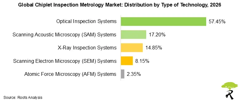
- Based on type of technology, the chiplet inspection metrology market forecast suggests that optical inspection systems hold the highest share at 57.45% in 2026. This dominance stems due to their established high-throughput role in semiconductor fabs, handling volume wafer and die inspections cost-effectively before advanced packaging stages.
- X-ray Inspection Systems will show robust growth, anticipated to grow at 25.2% CAGR through 2040. This unprecedented growth is driven by critical need for non-destructive subsurface void and crack detection in chiplet stacks and 2.5D / 3D interposers, where traditional optical falls short.
Regional Market Forecast: Asia-Pacific Holds the Largest Share
Based on our analysis, Asia-Pacific dominates at 48.70% chiplet metrology market share in 2026. This dominance is due to the fact that the manufacturing epicenter with TSMC / Samsung fabs ramping chiplet production. Some other notable chiplet inspection metrology industry growth drivers are mentioned below:
- Taiwan: TSMC has indeed solidified its "Advanced Packaging Leadership" through the aggressive expansion of its CoWoS (Chip-on-Wafer-on-Substrate) and SoIC (System-on-Integrated-Chips) platforms in the region with a planned capex of USD 52-56 billion in 2026. The core concentration of the company is focused on leading foundries and OSATs.
- South Korea: Samsung foundry expansion and SK Hynix’s HBM4 development is offering opportunities to market players for investments and partnerships in the region.
- China: "Made in China 2025" strategy driving domestic metrology tool development; for instance, Hua Hong USD 2.95B facility investment.
- Japan: Japan’s strength in automotive semiconductors (led by giants like Renesas and Sony) is pushing chiplet metrology toward extreme reliability. Modern vehicles are moving toward zonal architecture that combine 5nm / 7nm AI chiplets for self-driving with older, robust 28nm / 40nm chiplets for power management. Inspecting the interconnects between these diverse nodes is a massive growth area for metrology.
North America Chiplet Inspection Metrology Market Revenue Forecast
Based on the, chiplet yield management solutions market report, North America grows fastest at 24.3% CAGR through 2040. With USD 6.6 billion in grants to TSMC for US-based fabs and additional funding for Intel and Samsung, the US is aiming to onshore the entire optical inspection systems for advanced packaging value chain. This has created a fertile ground for domestic metrology innovation, particularly in AI-driven software and X-ray systems. In addition, the early adoption of next-generation metrology for leading-edge nodes; R&D collaboration hubs is driving the market growth. Several other growth catalysts are listed below:
- CHIPS and Science Act: USD 52B+ funding driving domestic fab construction.
- Intel 18A / 20A Nodes: Backside power delivery and RibbonFET adoption is driving the market expansion in this region.
- Hyperscaler Investments: Google, Amazon, Microsoft are driving the n-house chip development, which significantly pushing market players for investments and partnerships.
- Arizona / New Mexico / Texas Clusters: TSMC, Intel, and Samsung expansion into the US chiplet inspection metrology market, driving opportunities for the innovations.
Have Questions? Let's Get Them Answered
Market Ecosystem Insights
Chiplet Inspection Metrology Competitive Landscape and Market Share Analysis
The chiplet inspection metrology market is a central component of the global effort to secure semiconductor supply chains and achieve technological sovereignty. Overall, the market is immensely competitive, featuring the presence of tech giants and startup companies who are focused on structural shifts toward 3D integration, and "Discovery at the Speed of Light", the rare combination of atomic-scale sensitivity and industrial-scale throughput. Some of the notable examples of market players include Applied Materials, Camtek, Hitachi High-Tech, Onto Innovation, EV Group, Omron, Keyence, and Nearfield Instruments.

Global Chiplet Inspection Market Trends
- Integration of Artificial Intelligence and Machine Learning for Defect Classification: AI and ML algorithms offer significant opportunities to enhance defect identification and classification, moving beyond manual review of complex inspection data. By implementing predictive analytics, companies can forecast potential yield issues based on subtle process variations, enabling proactive adjustments to improve efficiency and reduce the need for human intervention.
- Expansion into High-Reliability Verticals (Automotive and Aerospace): While HPC and AI currently drive the market, automotive electronics (especially for ADAS and autonomous driving) and aerospace/defense applications are emerging high-value segments for chiplet technology. These verticals demand extremely high reliability and zero-defect tolerance, creating a strong market opportunity for advanced metrology tools that ensure mission-critical integrity.
- Development of Integrated In-line Metrology Solutions: Current metrology often relies on batch processing or standalone tools. There is an opportunity for inspection solution providers to integrate their systems directly into the advanced packaging assembly line, offering real-time, in-line process monitoring and feedback. This minimizes cycle time, reduces material handling, and provides immediate control over critical process parameters.
Get an Instant Quote in 10 Minutes. Lowest Price Guaranteed
Chiplet Inspection Metrology Market: Scope of the Report
| Key Report Attributes | Details | |
| Forecast Period | Till 2040 | |
| Market Size 2028 | $ 0.71 Billion | |
| Market Size 2040 | $ 12.80 Billion | |
| CAGR (Till 2040) | 22.94% | |
| Segments Covered |
|
|
Market Segmentation
Based on research, we have segmented the Chiplet Inspection Metrology Market, 2026-2040, into type of component, type of technology, type of measurement parameter, type of process, application area, end user, geographical regions, and key players.
Market Share by Type of Component
- Chiplets / Dyes
- Interposers
- Assembled Packages
Market Share by Type of Technology
- Optical Inspection Systems
- Scanning Acoustic Microscopy (SAM) Systems
- X-Ray Inspection Systems
- Scanning Electron Microscopy (SEM) Systems
- Atomic Force Microscopy (AFM) Systems
Market Share by Type of Measurement Parameter
- Critical dimension (CD) and Overlay Metrology
- Thin film and Surface Roughness Analysis
- 3D Metrology for Stacking and Interconnects
Market Share by Type of Process
- Pre-Assembly Inspection
- Post-Assembly Inspection
- Failure Analysis and R&D
Market Share by Application Area
- Wafer / Chiplet Inspection and KGD Testing
- Advanced Packaging Metrology
- Hybrid Bonding
- Interposers
- High-Performance Computing (HPC)
- AI
- Edge and Subsurface Defect Detection
Market Share by End Use Industry
- Automotive Electronics
- Aerospace and Defense
- Consumer Electronics
- Data Centers
- Industrial Automation
Market Share by Geographical Regions
- North America
- US
- Canada
- Mexico
- Rest of North America
- Europe
- Austria
- Belgium
- Denmark
- France
- Germany
- Ireland
- Italy
- Netherlands
- Norway
- Russia
- Spain
- Sweden
- Switzerland
- UK
- Rest of Europe
- Asia-Pacific
- Australia
- China
- India
- Japan
- New-Zealand
- Singapore
- South Korea
- Rest of Asia-Pacific
- Latin America
- Brazil
- Chile
- Colombia
- Venezuela
- Rest of Latin America
- Middle East and Africa (MEA)
- Egypt
- Iran
- Iraq
- Israel
- Kuwait
- Saudi Arabia
- UAE
- Rest of MEA


